
What are the Best Practices for PCB Prototype Assembly?
Printed Circuit Boards (PCBs) are the pulse of present day electronics, whether in smart phones, medical devices, or mechanical gear. Some time recently a item hits full-scale generation, it frequently goes through a few rounds of prototype assembly. PCB prototype assembly is the basic stage where thoughts meet reality, and indeed minor slips can lead to costly delays or item failures.
To ensure success, embracing best practices amid prototype assembly is vital. Let’s jump profound into the key steps and tips that can make or break your PCB project.
1.Start with a Clear and Nitty gritty Design
Every fruitful PCB prototype begins with a strong Design. Clear schematics, well-organized component libraries, and coherent board formats are basic. Architects must utilize up-to-date Electrical Computer-Aided Design (ECAD) devices such as Altium Originator, KiCAD, or Eagle.
Key points:
- Double-check the schematic for mistakes some time recently moving to the layout.
- Keep your Design straightforward; prioritize clarity over compactness in prototypes.
- Use legitimate Design for manufacturability (DFM) rules to maintain a strategic distance from issues later.
- Include test focuses and investigating highlights on the board.
Tip: Run a Design Rule Check (DRC) some time recently finalizing the Design to capture dividing, clearance, or layer issues early.
2.Select the Right PCB Materials
The choice of fabric influences your prototype’s strength, fetched, and execution. For most standard applications, FR4 fabric is a solid and cost-effective choice. In any case, for high-frequency or high-speed circuits, you might require specialized substrates like Rogers laminates.
Best hones for fabric selection:
- Evaluate warm, mechanical, and electrical properties based on your application.
- Consult with your constructing agent to guarantee fabric compatibility with their processes.
- Factor in costs: Prototype Boards may require diverse fabric methodologies than last production.
Tip: If you’re uncertain, begin with standard FR4 for your early prototypes to diminish costs.
3.Collaborate Closely with Your PCB Producer and Assembler
Open communication with your fabricating and assembly accomplices can anticipate numerous issues. Experienced accomplices frequently spot potential Design blemishes and suggest improvements.
Steps to follow:
- Share Gerber records, Charge of Materials (BOM), pick-and-place records, and assembly drawings in standardized formats.
- Ask for a Design for Assembly (DFA) audit some time recently production.
- Understand the capabilities and restrictions of your constructing agent, particularly for progressed innovations like microvias or fine-pitch components.
Tip: Set up a input circle. The assembler’s bits of knowledge can altogether progress the Design in consequent prototype iterations.
4.Optimize the Bill of Materials(BOM)
A clean, clear, and well-optimized BOM spares time and dodges disarray amid assembly. Make beyond any doubt your BOM includes:
- Correct portion numbers (producer and provider codes).
- Clear component descriptions.
- Quantity and designators coordinating the PCB layout.
- Alternative portion proposals for basic components.
Tip: Utilize common, promptly accessible components to speed up obtainment, particularly in the prototype stage when sourcing delays can affect timelines.
5.Component Arrangement and Orientation
Proper component arrangement and introduction are vital for useful and manufacturable PCBs. Components ought to be situated consistently to guarantee productive flag stream and less demanding debugging.
Placement best practices:
- Place high-speed or touchy components near to connectors or basic paths.
- Keep polarized components (e.g., diodes, electrolytic capacitors) clearly stamped and situated uniformly.
- Avoid setting components as well near to PCB edges unless completely necessary.
Tip: Gather comparable components together where possible—it makes a difference in robotized arrangement and manual inspection.

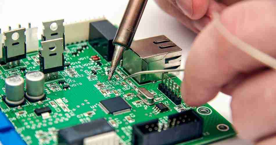
6.Pay Consideration to Fastening Techniques
In PCB prototype assembly, destitute patching is a common cause of useful disappointments. Whether you’re utilizing manual patching for a few Boards or a reflow broiler for group prototypes, exact patching hones must be followed.
Soldering recommendations:
- Use the adjust patch glue sort and stencil thickness for the components.
- Maintain reliable temperature profiles amid reflow to anticipate absconds like tombstoning or cold joints.
- For hand fastening, guarantee administrators are IPC-certified or well-trained.
Tip: For fine-pitch components like QFNs or BGAs, dodge manual fastening if conceivable. Utilize reflow patching with proficient gear for best results.
7.Careful Review and Testing
Prototype PCBs must be reviewed completely after assembly. This step catches surrenders early some time recently they cascade into greater issues amid useful testing.
Inspection techniques:
- Visual Assessment: Manual checking beneath magnification.
- AOI (Automated Optical Inspection): Machines filter for arrangement, lost components, patch bridges, etc.
- X-ray Review: Fundamental for covered up joints like those beneath BGAs.
Tip: Indeed if you utilize AOI, a last manual assessment is astute for catching irregularities that machines might miss.
8.Include Test Points for Debugging
During prototyping, it’s not about just making the board work once—it’s about understanding why it works (or doesn’t). Test points are critical.
How to implement:
- Provide accessible test points for key nets like power, ground, clocks, and critical signals.
- Use test pads or small vias designed specifically for oscilloscope probes.
- Label test points clearly to speed up troubleshooting.
Tip: Allocate space for a debug connector (like a JTAG or UART header) if your circuit includes programmable devices.
9.Validate the Prototype Thoroughly
Once the board powers up successfully, deeper validation is needed. Check not only if the board works but if it performs within specifications.
Validation checklist:
- Measure power rails for correct voltages.
- Verify signal integrity for high-speed lines.
- Test thermal performance under load conditions.
- Validate software integration if the PCB interfaces with firmware.
Tip: Document all findings meticulously—it’ll make redesigns and iterations much easier.
10.Prepare for Iterations
Rarely does the first prototype get everything right. Expect a few iterations.
Best practices for iteration:
- Record all design changes based on prototype feedback.
- Implement Engineering Change Orders (ECOs) methodically.
- Keep track of revision numbers clearly in all files (Gerbers, BOMs, layouts).
Tip: Start with a small batch of prototypes before scaling up production based on validated designs.
11.Consider Using Turnkey PCB Assembly Services
For startups, small teams, or solo engineers, turnkey PCB assembly services can simplify the process greatly. These services handle sourcing, assembly, and basic testing.
Why consider turnkey services:
- Speed: Faster time to functional boards.
- Quality: Professional handling reduces assembly errors.
- Convenience: One-stop-shop from order to delivery.
Tip: Ensure your turnkey partner can handle the complexity of your design—especially if it involves fine-pitch components or advanced PCB technologies.
Conclusion
PCB prototype assembly is much more than fair putting components on a board. It’s a carefully coordinated prepare including Design perseverance, fabric determination, collaboration, exactness fastening, and thorough testing. Each choice made amid this stage impacts the victory of the last product.
By taking after these best hones, you can decrease chance, spare time and cash, and quicken the travel from thought to reality. A prototype is not fair a test board—it’s a establishment stone for the product’s future.
Latest Blog


Table of Content
Contcat Us
Phone: +86-18123905375
Email: sales@circuitcardassembly.com
Skype: ali_youte
WhatsApp: +86-18123905375
Wechat: +86-18123905375

 Afrikaans
 Shqip
Shqip አማርኛ
አማርኛ العربية
 Հայերեն
 Azərbaycan dili
 Euskara
 Беларуская мова
 বাংলা
বাংলা Bosanski
 Български
 Català
 Cebuano
 Chichewa
 简体中文
简体中文 繁體中文
繁體中文 Corsu
Corsu Hrvatski
 Čeština
 Dansk
Dansk Nederlands
 Esperanto
 Eesti
Eesti Filipino
 Suomi
Suomi Français
 Frysk
Frysk Galego
 ქართული
 Deutsch
 Ελληνικά
 ગુજરાતી
 Kreyol ayisyen
 Harshen Hausa
 Ōlelo Hawaiʻi
 עִבְרִית
 हिन्दी
 Hmong
Hmong Magyar
 Íslenska
 Igbo
Igbo Bahasa Indonesia
 Gaeilge
 Italiano
 日本語
日本語 Basa Jawa
 ಕನ್ನಡ
ಕನ್ನಡ Қазақ тілі
 ភាសាខ្មែរ
 한국어
한국어 كوردی
كوردی Кыргызча
 ພາສາລາວ
 Latin
Latin Latviešu valoda
 Lietuvių kalba
 Lëtzebuergesch
 Македонски јазик
 Malagasy
 Bahasa Melayu
 മലയാളം
 Maltese
 Te Reo Māori
 मराठी
मराठी Монгол
 ဗမာစာ
ဗမာစာ नेपाली
 Norsk bokmål
 پښتو
پښتو فارسی
فارسی Polski
 Português
 ਪੰਜਾਬੀ
 Română
 Русский
 Samoan
 Gàidhlig
 Српски језик
 Sesotho
 Shona
Shona سنڌي
سنڌي සිංහල
සිංහල Slovenčina
 Slovenščina
 Afsoomaali
 Español
 Basa Sunda
 Kiswahili
 Svenska
 Тоҷикӣ
 தமிழ்
தமிழ் తెలుగు
 ไทย
ไทย Türkçe
 Українська
 اردو
اردو O‘zbekcha
 Tiếng Việt
 Cymraeg
 isiXhosa
 יידיש
יידיש Yorùbá
 Zulu
Zulu